


 33 / 100

February 2016
33
Technical
it will probably go right through the board.
Photo 3
shows the top of the board at this
stage.
Assembly
The board was populated using standard
0.25W resistors and 100nF ceramic disc
capacitors. T1 is 10 turns, bifilar wound on a
small ferrite toroid (FT37-43 or similar) using
two lengths of enamelled copper twisted
together. I used 0.375mm wire, although the
exact diameter is not that critical. No heatsink
is required for the transistor. A close-up of the
assembled circuit is shown in
Photo 4
.
Attenuator stages
Two switched amplifiers allow for gain of
0, 20 and 40dB. Adding a pair of switched
attenuators will allow greater control of
gain, input level, and input return-loss. Any
practical value of attenuation can be used.
I have chosen 10dB and 20dB for my
project. The attenuators are based on the
standard PI configuration.
Table 1
shows
ideal component values for several different
attenuation values. In some cases, it may
be acceptable to substitute the nearest
standard value, eg 18Ω instead of 17.6Ω.
Where greater accuracy is required, it may
be necessary to make up the required
value using combinations of standard
values, eg 22Ω in parallel with 91Ω =
(22×91)÷(22+91) = 17.71Ω.
Figure 2
shows the pi configuration and component
values for a 20dB attenuator using parallel
pairs of standard resistors. Suggested values
for the 10dB version are 100Ω || 2700Ω
= 96.4Ω and 82Ω || 560Ω = 71.5Ω.
There is little to be gained from accuracy
beyond 1%. This is the closest tolerance that
is readily available and in any case, a real-
world source or load circuit is unlikely to be
a perfect 50Ω. The wiring of the combined
attenuator/amplifier is shown in
Figure 3.
The switches are standard DPDT types.
Testing
As expected, the attenuators perform
accurately from LF to VHF. The bandwidth of
this unit will be limited by the performance of
the amplifiers. Amplifier
gain was measured at
40dB using a signal
generator and several
different
detectors,
including a spectrum
analyser, oscilloscope
and, at higher output,
a simple diode probe.
1dB bandwidth extends
from 1MHz to 40MHz.
The -3dB points are at
400kHz and 60MHz.
This is perfect for MF-HF
and still useful at 6m.
Other types of
construction
Apart from etched PCBs,
there are many other
types of construction
used by radio amateurs.
Perforated stripboard,
with or without copper
tracks
(Veroboard)
and various types of
IC prototyping boards
are basically generic or
universal forms of PCB. Various point-to-
point wiring schemes are in widespread use.
Many of these pre-date the PCB. The original
breadboard was probably just a wooden
board with copper nails for connections.
Modern plug-in breadboards are based on
a 0.1in matrix. Once the design is tested, it
is easily transferred to 0.1in Veroboard for a
more reliable and durable circuit.
Point-to-point wiring systems generally
use a few anchor points for mechanical
stability. Most of the circuit connections
are made by soldering component leads
together or by short wire links. Several
named variants have evolved: dead bug,
ugly construction, Manhattan and so on.
Regular readers will know that I usually build
prototypes on copper PCB laminate. This
produces a reasonably strong, durable and
stable circuit. I have used various types of
anchor points, including push-through PTFE
stand-off insulators, screw or bolt mounted
ceramic pillars and tag-strip (which was very
popular in the valve era). In most cases, I find
it is possible to build a solid circuit without
the need for expensive and inaccessible
hardware. Most circuits will have several
points connected to the ground foil as part of
the electrical design. Decoupling capacitors
are convenient anchor points. In those cases
where a dedicated stand-off is required, a
10MΩ resistor costs around 1p and, for most
purposes, is an almost perfect insulator.
RF signal source
Our final project for this month is an RF
signal source. This is easily built for any LF-
HF frequency where a suitable fundamental
mode crystal is available. I have chosen
10MHz as a good test frequency because it
is near the centre of the HF range and I have
a good stock of 10MHz crystals. RF output
is -30dBm (or 1μW). This can be reduced
using a step attenuator for weak signal
testing or increased to a higher level using
the amp/attenuator described earlier.
The schematic is shown in
Figure 4
. The
oscillator is based on an MPSH10 transistor.
The assembled unit is shown in
Photo 5
. I
used a strip of SS PCB laminate as a base
for the circuit. All ground connections are
directly to the copper foil. Components are
deliberately arranged to provide stand-off
supports. The Zener diode and decoupling
capacitor at top-centre are a typical example.
Eamon Skelton, EI9GQ
hbradio@eircom.netVcc+
Vcc+
-10dB switch
-20dB switch
+20dB switch
+20dB switch
In
Out
FIGURE 2:
General arrangement of switched attenuators and amplifiers.
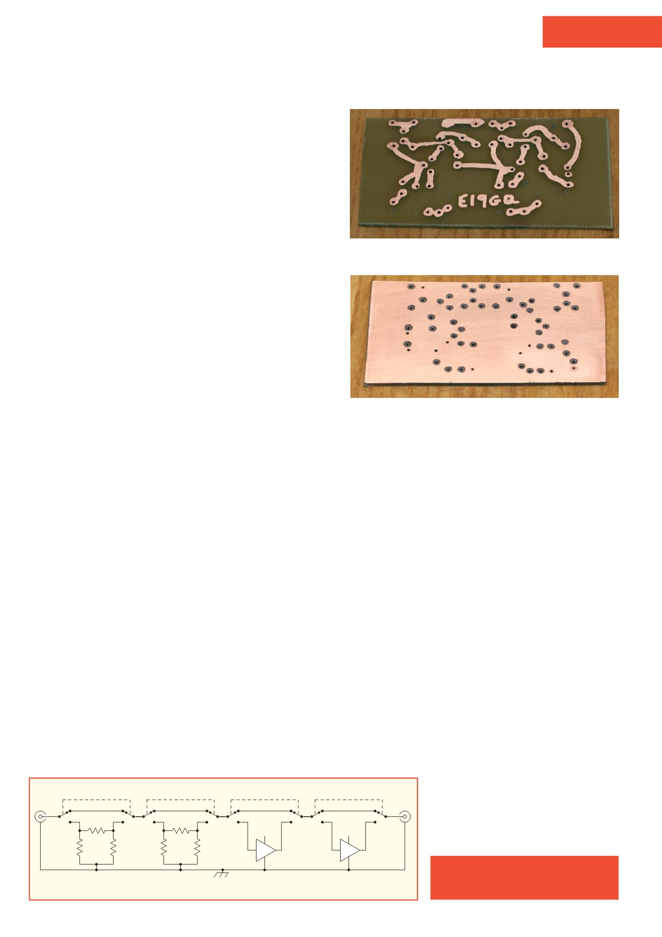
PHOTO 3:
Top (ground plane) side of the PCB after removing copper
from non-grounded holes.
PHOTO 2:
Track side of the PCB.