


 32 / 100

February 2016
32
M
any of the circuits used
in radio equipment are
relatively simple. A typical
design will have multiple stages,
each of which can be considered
as a separate block. This
modular approach to design and
construction means that there are
only a few connections required
between each block. In the case of
an amplifier: power supply, input,
output and ground. Such simple
circuits are easily accommodated
on a single-sided PCB layout.
Double sided boards
For more complex circuits, it may be difficult
to find ideal routes for all PCB traces on a
single-sided board without using wire links
or extra components to bridge the gap where
one trace must cross another. In some cases,
PCB designers will include unnecessary
components or dummy devices like the
‘zero-ohm resistor’ to create gaps for other
traces to pass through. Double-sided and
multi-layer PCBs give the board designer
more routing options than a single-sided
design. This reduces the need for wire links
and unnecessary components. Multi-layer
boards can also offer superior performance,
particularly in high frequency circuits where
having separate layers for ground, power and
signals can reduce noise. Double sided and
multi-layer boards allow wider circuit traces
for a given board area. This reduces resistance
and inductance. The ability to designate areas
of copper as a heatsink can also improve
component reliability.
Last month, we looked at several different
methods for producing single-sided (SS)
PCBs. The same techniques can also be
applied to the production of double-sided (DS)
boards. In most cases, DS boards are made
using double-sided PCB laminate, although
I have also made boards from a pair of thin
SS laminates that were etched separately and
then bonded together using epoxy adhesive.
The resulting board was the same thickness
as standard 1.6mm PCB.
For home produced DS boards, the most
common approach is to use a DS PCB
laminate. It is possible to apply the resist
and etch both sides of the board at the same
time. I find it much easier to do each side as a
separate process. Etch resist is applied to one
side of the board using any of the methods
described last month. The other side is
masked from the etchant using a coat of paint
or a few overlapping strips of plastic tape. The
board is then etched in the normal way. After
etching and cleaning the board, the mask is
removed from the other side. Etch resist is
applied to the second side, a new mask is
applied to the previously etched side and the
board is placed in the etchant for a second
time. For most designs, accurate alignment
of the two sides is critically important. Most
PCB CAD layouts show the board outline and
special alignment marks for this purpose.
In the distant past, I used aerosol car paint
or clear lacquer as the etchant mask. This
makes an excellent mask as it is absolutely
waterproof. Drying time for the two sides
adds at least an hour to the full process. After
etching, the mask could be removed using
paint stripper. I find this is getting progressively
more difficult as the new formulas for paint
stripper seem quite ineffective. I now use
overlapping strips of PVC insulating tape,
as shown in
Photo 1
. This is very effective
provided you drive out air bubbles and make
sure there are no gaps where the etchant
can reach the copper foil. This method is
much quicker than painting because there is
no drying time and the mask is very easily
removed.
RF amplifier/attenuator
One type of double-sided board that is very
effective for HF to UHF circuits uses one
complete side of the board as a continuous
ground plane. Ground connections are made
by soldering the component leads directly to
the top foil. The area around holes for non-
grounded component leads is cleared of
copper. This is achieved by etching or, more
commonly at home, by countersinking the
hole using a larger drill bit as a hand tool.
Signal and power traces are on the opposite
side of the PCB. As a simple project, we will
make a HF amplifier using this technique. As
I often have need for a 50Ω adjustable gain
block, this two stage amplifier will be used
in combination with a pair of 50Ω switched
attenuators to make a useful bench amplifier
with gain/loss adjustable in 10dB steps
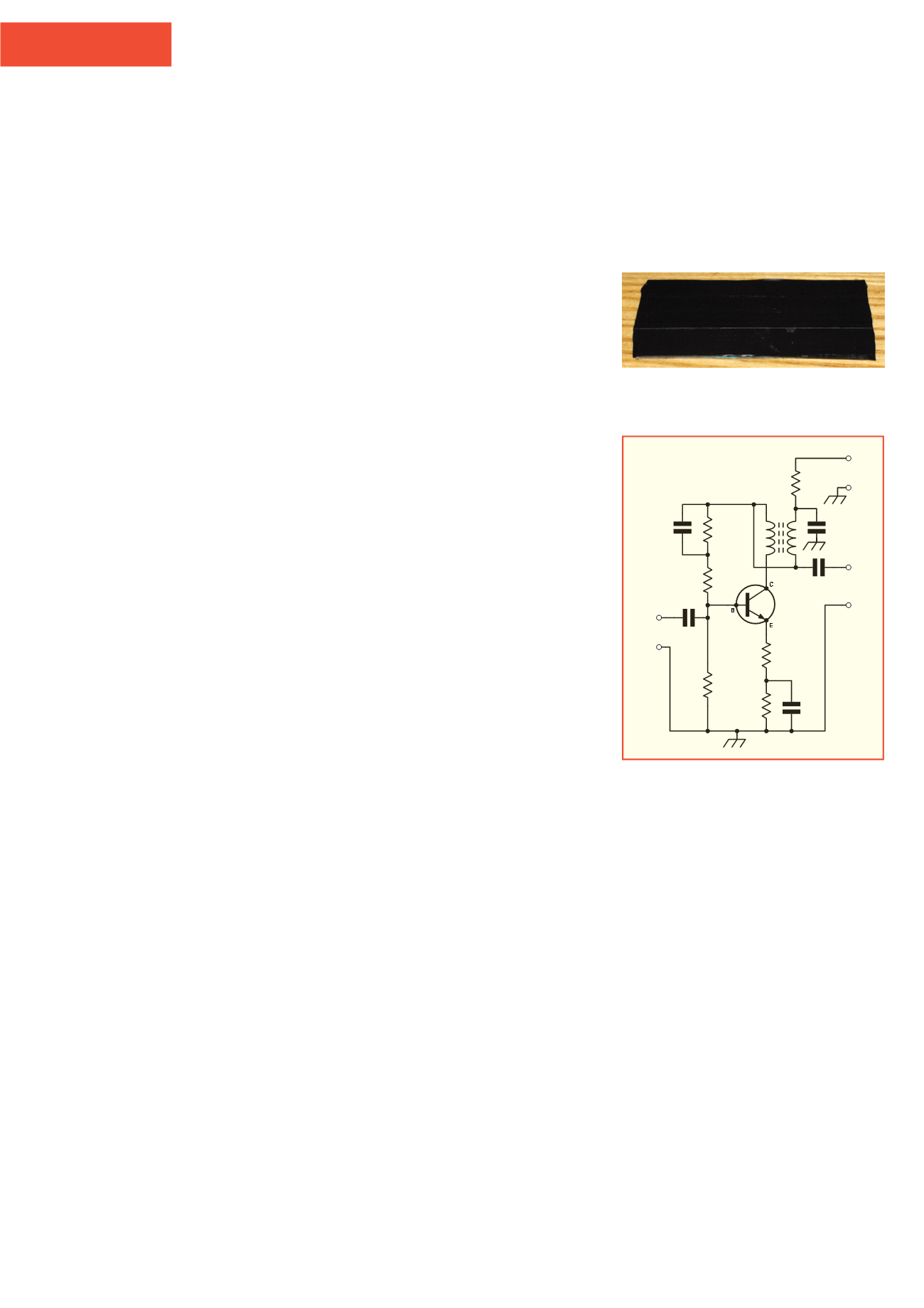
from -30dB to +40dB. The schematic for
each amplifier stage is shown in
Figure 1
.
Component values are chosen for a stage gain
of 20dB.
The resist was applied by hand using a
standard etch-resist pen. I used a printout of
a PCB CAD layout as a reference. The holes
were drilled before applying the etch-resist so
that they could be used as a guide for drawing
the tracks. After drilling, the copper was
cleaned and flattened using wet or dry paper.
This is important because an uneven surface
could allow etchant to enter the masked side
via the drill holes. The resist was left to dry
for one hour before masking and etching. I
used a few strips of PVC insulating tape as a
mask for the top side.
The board was etched using a ferric
chloride solution and washed off with clean
water. The track side (bottom) is shown in
Photo 2
: not pretty, but perfectly functional.
Note that there is no copper around some
of the holes. These are for leads that are
soldered to the ground foil on the other side.
The holes were drilled with a 0.9mm drill
and I used a new and sharp 5mm HSS bit
as a hand tool to remove copper from around
each non-ground connection on the top of
the board. You only need to make one or
two turns of the drill bit to remove sufficient
copper. Don’t use a power drill for this, as
Homebrew
Technical
MPSH10
4Ω7
100Ω
0 1
1k
510Ω
3k3
0 1
0 1
In
T1
0 1
56Ω
0 1
DC
Out
FIGURE 1:
50Ω amplifier
stage (see text).
PHOTO 1:
Using strips of PVC masking tape as
an etchant mask.